Micro PMU with 1.2 A Buck, Two 300 mA LDOs,
Supervisory, Watchdog, and Manual Reset
Data Sheet
ADP5041
Rev. 0
Information furnished by Analog Devices is believed to be accurate and reliable. However, no
responsibility is assumed by Analog Devices for its use, nor for any infringements of patents or other
rights of third parties that may result from its use. Specifications subject to change without notice. No
license is granted by implication or otherwise under any patent or patent rights of Analog Devices.
Trademarks and registered trademarks are the property of their respective owners.
One Technology Way, P.O. Box 9106, Norwood, MA 02062-9106, U.S.A.
Tel: 781.329.4700
www.analog.com
Fax: 781.461.3113
?SPAN class="pst ADP5041ACPZ-1-R7_2473529_0">2011 Analog Devices, Inc. All rights reserved.
FEATURES
Input voltage range: 2.3 V to 5.5 V
One 1.2 A buck regulator
Two 300 mA LDOs
20-lead, 4 mm ?4 mm LFCSP package
Overcurrent and thermal protection
Soft start
Undervoltage lockout
Open-drain processor reset with externally adjustable
threshold monitoring
Guaranteed reset output valid to VAVIN = 1 V
Manual reset input
Watchdog refresh input
Buck key specifications
Output voltage range: 0.8 V to 3.8 V
Current mode topology for excellent transient response
3 MHz operating frequency
Peak efficiency up to 96%
Uses tiny multilayer inductors and capacitors
Mode pin selects forced PWM or auto PWM/PSM mode
100% duty cycle low dropout mode
LDOs key specifications
Output voltage range: 0.8 V to 5.2 V
Low input supply voltage from 1.7 V to 5.5 V
Stable with 2.2 糉 ceramic output capacitors
High PSRR
Low output noise
Low dropout voltage
40癈 to +125癈 junction temperature range
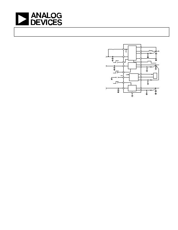
FUNCTIONAL BLOCK DIAGRAM
SW
EN_BK
FB2
R4
R4
R5
R3
FB3
R3
R7
C5
2.2礔
C6
2.2礔
VOUT2
AVIN
VBIAS
VBIAS
VOUT1
FB1
L1
1礖
R1
R2
V
IN1
= 2.3V TO
5.5V
C1
4.7礔
SUPERVISOR
礟
nRSTO
WDI
VTHR
MR
R
FILT
= 30&
V
IN2
= 1.7V
TO 5.5V
VIN1
ON
OFF
ON
OFF
ON
OFF
EN1
VIN2
C2
1礔
C3
1礔
EN2
EN3
VIN3
V
IN3
= 1.7V
TO 5.5V
EN_LDO2
LDO2
(ANALOG)
BUCK
AGND
V
OUT1
AT
1.2A
C6
10礔
PGND
FPWM
PSM/PWM
MODE
V
OUT2
AT
300mA
V
OUT3
AT
300mA
VOUT3
LDO1
(DIGITAL)
EN_LDO1
Figure 1.
GENERAL DESCRIPTION
The ADP5041 combines one high performance buck regulator
and two low dropout regulators (LDO) in a small 20-lead
LFCSP to meet demanding performance and board space
requirements.
The high switching frequency of the buck regulator enables
use of tiny multilayer external components and minimizes
board space.
When the MODE pin is set to logic high, the buck regulator
operates in forced PWM mode. When the MODE pin is set to
logic low, the buck regulator operates in PWM mode when the
load is around the nominal value. When the load current falls
below a predefined threshold, the regulator operates in power
save mode (PSM), improving the light load efficiency. The low
quiescent current, low dropout voltage, and wide input voltage
range of the ADP5041 LDOs extend the battery life of portable
devices. The ADP5041 LDOs maintain a power supply rejection
greater than 60 dB for frequencies as high as 10 kHz while
operating with a low headroom voltage.
Each regulator in the ADP5041 is activated by a high level on
the respective enable pin. The output voltages of the regulators
and the reset threshold are programmed through external resistor
dividers to address a variety of applications. The ADP5041
contains supervisory circuits that monitor power supply voltage
levels and code execution integrity in microprocessor-based
systems. They also provide power-on reset signals. An on-chip
watchdog timer can reset the microprocessor if it fails to strobe
within a preset timeout period.
发布紧急采购,3分钟左右您将得到回复。
相关PDF资料
ADP5042ACPZ-2-R7
IC REG TRPL BCK/LINEAR 20LFCSP
ADT6402SRJZ-RL7
IC TEMP SENS TRIP PT PP SOT-23-6
ADT6501SRJZP085RL7
IC TEMP SENSOR MICROPWR SOT23-5
ADT7302ARTZ-500RL7
IC SENSOR TEMP 13BIT DGT SOT23-6
ADT7310TRZ
IC TEMP SENSOR 16BIT SPI 8SOIC
ADT7461AARMZ-R
IC TEMP SENSOR DGTL 2CH 8-MSOP
ADT7461ARMZ-2R
IC TEMP SENSOR DGTL 2CH 8-MSOP
ADT7463ARQZ-REEL
IC REMOTE THERMAL CTRLR 24-QSOP
相关代理商/技术参数
ADP5041CP-1-EVALZ
功能描述:ADP5041 - DC/DC, Step Down with LDO 3, Non-Isolated Outputs Evaluation Board 制造商:analog devices inc. 系列:- 零件状态:有效 主要用途:DC/DC,LDO 步降 输出和类型:3,非隔离 功率 - 输出:- 电压 - 输出:- 电流 - 输出:1.2A,300mA,300mA 电压 - 输入:2.3 V ~ 5.5 V 稳压器拓扑:降压 频率 - 开关:3MHz 板类型:完全填充 所含物品:板 使用的 IC/零件:ADP5041 标准包装:1
ADP5042
制造商:AD 制造商全称:Analog Devices 功能描述:Micro PMU with 0.8 A Buck, Two 300 mA LDOs Supervisory, Watchdog and Manual Reset
ADP5042ACPZ-1
制造商:Analog Devices 功能描述:PMU 2 LDO DUAL BUCK 20LFCSP 制造商:Analog Devices 功能描述:PMU, 2 LDO, DUAL BUCK, 20LFCSP
ADP5042ACPZ-1-R7
功能描述:IC REG TRPL BCK/LINEAR 20LFCSP RoHS:是 类别:集成电路 (IC) >> PMIC - 稳压器 - 线性 + 切换式 系列:- 标准包装:2,500 系列:- 拓扑:降压(降压)同步(3),线性(LDO)(2) 功能:任何功能 输出数:5 频率 - 开关:300kHz 电压/电流 - 输出 1:控制器 电压/电流 - 输出 2:控制器 电压/电流 - 输出 3:控制器 带 LED 驱动器:无 带监控器:无 带序列发生器:是 电源电压:5.6 V ~ 24 V 工作温度:-40°C ~ 85°C 安装类型:* 封装/外壳:* 供应商设备封装:* 包装:*
ADP5042ACPZ-2
制造商:Analog Devices 功能描述:PMU 2 LDO DUAL BUCK 20LFCSP 制造商:Analog Devices 功能描述:PMU, 2 LDO, DUAL BUCK, 20LFCSP
ADP5042ACPZ-2-R7
功能描述:IC REG TRPL BCK/LINEAR 20LFCSP RoHS:是 类别:集成电路 (IC) >> PMIC - 稳压器 - 线性 + 切换式 系列:- 标准包装:2,500 系列:- 拓扑:降压(降压)同步(3),线性(LDO)(2) 功能:任何功能 输出数:5 频率 - 开关:300kHz 电压/电流 - 输出 1:控制器 电压/电流 - 输出 2:控制器 电压/电流 - 输出 3:控制器 带 LED 驱动器:无 带监控器:无 带序列发生器:是 电源电压:5.6 V ~ 24 V 工作温度:-40°C ~ 85°C 安装类型:* 封装/外壳:* 供应商设备封装:* 包装:*
ADP5042CP-1-EVALZ
功能描述:电源管理IC开发工具 Output Buck Regulator + Dual Fixed Eval RoHS:否 制造商:Maxim Integrated 产品:Evaluation Kits 类型:Battery Management 工具用于评估:MAX17710GB 输入电压: 输出电压:1.8 V
ADP5042CP-2-EVALZ
功能描述:电源管理IC开发工具 Output Buck Regulator + Dual Fixed Eval RoHS:否 制造商:Maxim Integrated 产品:Evaluation Kits 类型:Battery Management 工具用于评估:MAX17710GB 输入电压: 输出电压:1.8 V